

The scientific community is currently focused on the meticulous optimization of "tunnel junctions," which are the thin layers that connect the multiple active regions within a multi-junction laser chip. These layers must allow for the efficient flow of electrons while remaining transparent to the light being generated. Ongoing Multi Junction VCSEL Chips Market research is essential for identifying the materials and doping concentrations that minimize electrical resistance and optical absorption at these critical interfaces. For our group discussion, it is important to understand that the performance of the entire device is only as strong as its weakest junction. If the tunnel junctions are not perfectly tuned, the chip will suffer from "voltage drop" and excessive heating, which can lead to catastrophic failure. This high-precision engineering is what separates market leaders from those still struggling with low yields and inconsistent performance in their production lines.
Furthermore, the integration of "diffractive optical elements" (DOE) directly onto the laser aperture is opening new possibilities for beam shaping and pattern generation. This is particularly relevant for "structured light" applications, such as 3D facial scanning and secure biometric authentication. By combining the high power of a multi-junction design with the precision of integrated optics, manufacturers can create more robust sensing modules that work reliably even in bright sunlight. The industry is also seeing a push toward "wafer-level testing," where thousands of chips are characterized before they are even cut from the semiconductor wafer. This data-centric approach to quality control allows for the identification of subtle trends in the manufacturing process, enabling continuous improvement in yield and performance. As we refine these analytical and manufacturing methodologies, the cost of high-power photonics will continue to fall, paving the way for its integration into even the most cost-sensitive consumer applications.
FAQs
-
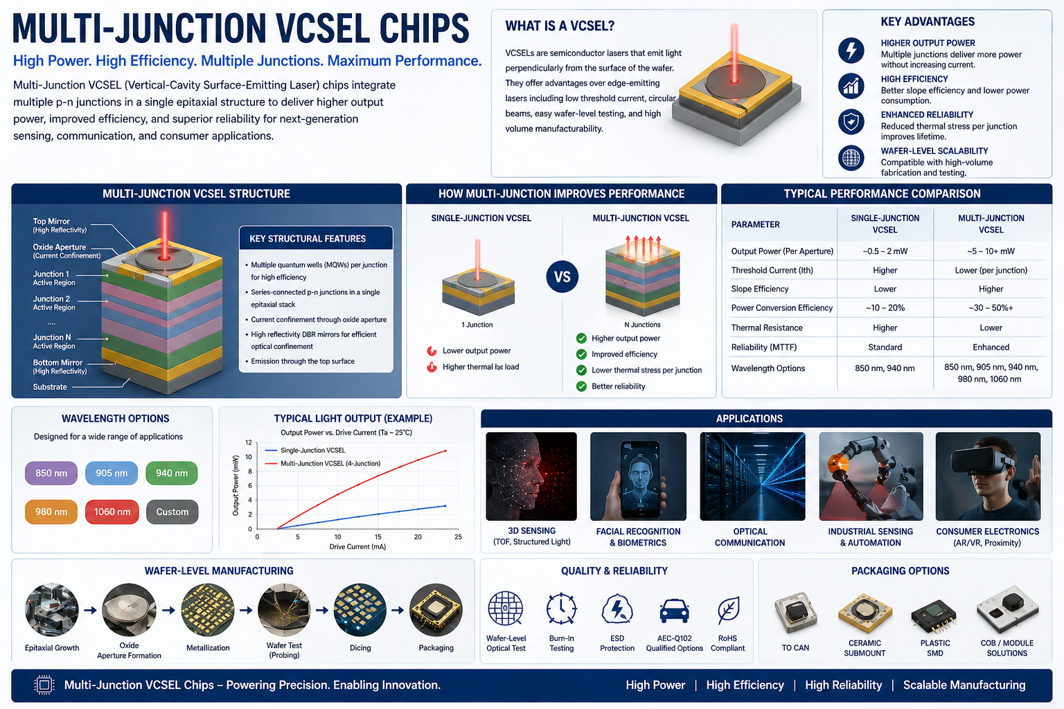
What is a tunnel junction in a VCSEL chip? It is a very thin, heavily doped layer that allows electrons to "tunnel" through a barrier, effectively connecting two active laser regions in a stack.
-
Why is 940nm a common wavelength for these chips? This wavelength is invisible to the human eye and experiences less interference from sunlight, making it ideal for outdoor sensing and mobile applications.